Patented fabrication flow
Click to enlarge

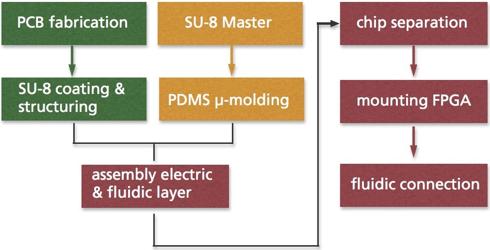
The right figure shows the whole fabrication process-flow of polyimide-based devices. The base material we used is a high performance polyimide laminate. This prepreg is favored because of the proven biocompatibility of polyimide. The main subprocess is the lithography step for structuring the SU 8 photoresist layer. The deposition of the polymer film has multiple functions. It acts as a planarization layer and isolates the conducting paths against the microfluidic channels. Furthermore the thin SU8 layer enables a defined opening at the positions of electrodes, conducting pads and the ball grid array as well as solder mask for FPGA packaging. Lastly it allows a homogeneous and irreversible sealing of PDMS microchannels and the PCB material. The resulting assembly is shown in the upper figure. The gold plated microelectrodes have dimensions down to 100 μm in width with a minimal spacing of 100 μm. Selective openings (60 x 60 μm) in SU 8 layer provide the contact areas with the biochemical fluids.
 Sectional representation of the fully assembled polyimide-based BioPCB.